


Abstract
Optical nanoantennas have attracted significant attention over the past decades, owing to their exceptional capabilities in terms of light manipulation and versatile optical applications. Recently, active nanoantennas have been developed by introducing phase change materials, to achieve specific tunable electromagnetic responses. However, most of these attempts only function with 'ON'/'OFF' states or switch in a few discrete states, significantly restricting the application in dynamic tunability. Thus far, the continuous and reversible modulation of optical nanoantennas has not been sufficiently explored. In this article, we experimentally demonstrate a continuously and reversibly electro-tunable optical nanoantenna, by integrating an asymmetric gold nanodisk dimer array with a vanadium dioxide (VO2) film and graphene thin film. By accurately controlling the applied electrical current, the Joule heat generated in the graphene film excites the metal-insulator phase transition of VO2, and the refractive index of VO2 exhibits a relatively large variation. When VO2 is in the insulating phase, we observe an apparent resonance dip in the reflection spectrum, which is attributed to a hybrid mode originating from the gap plasmon in the dimers and localized surface plasmon (LSP) resonance excited at the edge of the nanodisks. Meanwhile, owing to the coupling between two asymmetric LSP resonances in the neighboring nanodisks, the reflected peak based on the Fano effect is realized. However, once VO2 is in the metallic phase, the hybrid mode becomes weaker and red-shifted, and the Fano effect disappears. Thereafter, the continuous and reversible electro-modulation of the nanoantenna features, including the resonant wavelength, resonant intensity, and quality factors (Q), are experimentally verified in the optical communication region, by varying the applied electrical current in the hybrid structure. To further increase the modulation range of these properties, we scan the gap size and structural asymmetry parameter of the nanodisk dimer. The results show that, with a smaller gap size, the resonant intensity of the nanoantenna is stronger. When the structural asymmetry parameter increases, the resonant wavelength is redshifted. We expect that such continuously and reversibly electro-tunable nanoantennas will stimulate various applications in optical communication systems, tunable photoelectric sensors, and beyond.
Export citation and abstract BibTeX RIS

Original content from this work may be used under the terms of the Creative Commons Attribution 4.0 licence. Any further distribution of this work must maintain attribution to the author(s) and the title of the work, journal citation and DOI.
1. Introduction
Optical nanoantennas [1] play a crucial role in nanophotonics, because they can efficiently confine the electromagnetic fields at the sub-wavelength scale and manipulate the light radiation in the far-field [2]. To achieve the specific electromagnetic responses required by different applications, several types of nanoantennas have been proposed, including nanoparticle [3–7], nanorod [8–11], nanodisk [12–15], and bowtie [16–18] nanoantennas. Based on these designs, many optical metadevices have been demonstrated, such as photodetectors [19, 20], solar cells [21], sensors [22], and spectrometers [23]. However, most optical nanoantennas only operate with a static scheme, and their electromagnetic functionalities remain fixed after fabrication, limiting their further application in complex and changeable scenarios.
To overcome this problem, active nanoantennas [24, 25] have recently been developed, and have attracted much attention owing to their dynamic tunability. By combining their design with dynamically tunable elements, such as graphene [26], indium tin oxide [27], liquid crystals [28], and phase-change materials [29–37], the optical responses of nanoantennas can be dynamically controlled for different scenarios. Among the aforementioned dynamic designs, active optical nanoantennas based on the phase transition of VO2 are particularly fascinating [33, 34]. The optical properties of VO2 exhibit relatively large changes before and after the phase transition [38, 39], which can considerably enhance the dynamic tunability of fabricated optical devices [40, 41]. Consequently, active plasmonic optical nanoantennas [33] and active dielectric optical nanoantennas [34] can be realized based on VO2-integrated nanostructures. However, most of them can only work with 'ON'/'OFF' or several discrete states, which significantly restricts their applications in terms of dynamic tunability. Additionally, these devices usually utilize thermal modulation to control the phase transition process, which requires additional heating components, thereby increasing the complexity of the device. Therefore, continuously and reversibly electro-tunable optical nanoantennas based on VO2 are of considerable interest, but research on this topic remains lacking.
In this study, by integrating an asymmetric gold nanodisk dimer array with a VO2 film and a graphene thin film, we experimentally demonstrated the continuously and reversibly electro-tunable optical nanoantenna. In this composite metastructure, the reflected dip was attributed to a hybrid mode originating from the gap plasmon in the dimers and localized surface plasmon (LSP) resonance excited at the edge of the nanodisks, and the reflected peak was generated from the Fano effect, which refers to the coupling between two asymmetric LSP resonances in the neighboring nanodisks. By applying an electrical current, the Joule heat in the graphene could accurately control the phase transition of VO2, thereby realizing the electro-tuning resonance peak and dip of the optical nanoantenna. The experimental results showed that the continuous and reversible modulation of the properties of the nanoantenna, including the resonant wavelength, resonant intensity, and quality factor (Q-factor), were verified in the optical communication region, which agrees well with the theoretical design. Finally, we further varied the gap size and structural asymmetry parameter of the nanodisk dimer, to expand the modulation range. The results showed that the resonant intensity is stronger with a smaller gap size. Additionally, if the structural asymmetry parameter increases, the resonant wavelength undergoes a redshift. Our work provides a new method for realizing electrical-tunable optical nanoantennas that may potentially be applied in optical communication systems, tunable photoelectric sensors, and so on.
2. Theoretical design
We designed continuously and reversibly electro-tunable asymmetric dimer optical nanoantennas based on the phase transition material, VO2, as schematically shown in figure 1(a). To provide dynamic tunability, a 100 nm-thick VO2 film was designed on the glass substrate. Next, an asymmetric gold (Au) nanodisk dimer array was designed above the VO2 film. The dimer contained two Au nanodisks, and the connecting line of their centers was parallel to the x-direction, as schematically shown in figure 1(b). These two Au nanodisks had different diameters (240 nm on the left and 360 nm on the right) but the same thickness (20 nm), and the gap between the two Au nanodisks was set at 25 nm. Additionally, a 50 nm-thick silica (SiO2) film was used to separate the VO2 film and asymmetric Au nanodisk dimer arrays to reduce the electromagnetic loss [34]. The operating wavelength of our electro-tunable asymmetric dimer optical nanoantennas was designed to extend from 0.9 to 2.1 μm, covering the range of optical communication bands.

Figure 1. (a) Schematic of a continuously and reversibly electro-tunable asymmetric dimer optical nanoantenna, where the asymmetric Au nanodisk dimer array is placed between the SiO2 film and the graphene thin film. (b) Model of structural unit-cell; the dimer contains two Au nanodisks that have different diameters, but the same thickness. (c) Simulated reflection spectra of a VO2 film on a glass substrate when it is in insulating phase and metallic phase. (d) Simulated reflection spectra of an asymmetric dimer optical nanoantenna under x-polarized incidence when the VO2 film is in insulating phase and metallic phase.
Download figure:
Standard image High-resolution imageTo demonstrate the tunability of the optical properties of this device with the phase transition of the VO2 film, we first simulated the reflection spectra of a 100 nm-thick VO2 film on a glass substrate using finite-difference time-domain software (FDTD solutions, Lumerical Inc.). The refractive indices of the VO2 thin film in the insulating phase and metallic phase used for FDTD modeling were extracted from literature [38]. As shown in figure 1(c), the reflection spectra could undergo large changes at wavelengths from 0.9 to 2.1 μm, because of the change in the refractive index of VO2 before and after the phase transition. Next, we simulated the reflection spectra of the asymmetric dimer nanoantennas when VO2 was in the insulating phase and metallic phase, respectively. The periodicities of the dimer array were set to 800 and 600 nm along the x- and y-directions, respectively. The incident light was linearly polarized along the x-direction. In the simulation, the mesh was set to 2.5 nm along all three directions to obtain the electric field at each point. The refractive indices of Au and SiO2, which were used for FDTD modeling, were extracted from literature [42]. As shown in figure 1(d), the main reflected dip was observed at a wavelength of approximately 1.65 μm when VO2 was in the insulating phase, indicating a hybrid mode originating from the gap plasmon in the dimers and LSP resonance excited at the edge of the nanodisks. Furthermore, a reflected peak was observed, originating from the Fano effect due to the coupling between two asymmetric nanodisks. Conversely, when VO2 was in the metallic phase, the rightmost reflected dip undergoes an apparent red shift from 1.65 to 1.83 μm, indicating the dynamic modulation of the resonant wavelength. Additionally, the reflection decreased from 30.4% to 7.3%. Moreover, the reflected peak—due to the Fano effect—disappeared owing to the variation in the refractive index of the VO2 film. Consequently, the reflective intensity at the Fano resonance peak position decreased from 61.7% to 29.2%. These results verified the dynamic modulation of the resonant intensity for both the reflected dip and Fano resonance peak.
To explore the physical origin of the two modes that are shown in figure 1(d), we further simulated the in-plane electric field distributions for x-polarized incidence at the wavelengths around dip and peak positions. When VO2 was in the insulating phase, a reflected dip occurred at a wavelength of 1.65 μm. At this wavelength, the electric field was mainly concentrated at the gap between the leftmost and rightmost nanodisks, as shown in the top part of figure 2(a). Accordingly, the reflected dip occurred at 1.65 μm originated from the hybrid mode containing of gap plasmon and LSP mode. It was found that the electric field in the gap was significantly enhanced and the maximum electric field enhancement rate was approximately 23.8. When VO2 changed to the metallic phase, the reflected dip redshifted from 1.65 to 1.83 μm, which indicated this hybrid mode occurred at a wavelength of 1.83 μm as shown in the middle part of figure 2(a). And the maximum electric field enhancement rate was approximately 29.1 in this case. To better understand the phase transition's influence on the electric field distribution, we further simulated the in-plane electric field distributions at 1.83 μm when VO2 was in the insulating phase, as shown in the bottom part of figure 2(a). A maximum electric field enhancement rate of only 14.8 was observed under this condition, indicating no obvious mode was excited.
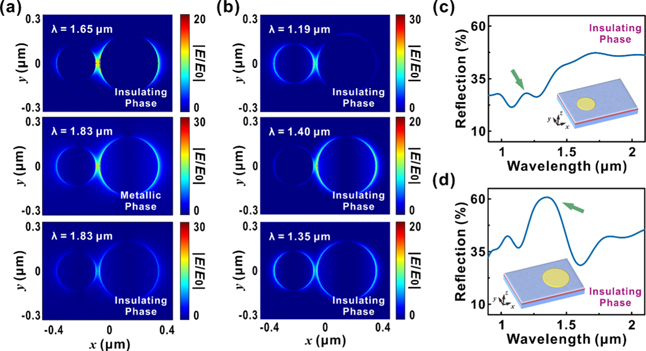
Figure 2. (a) In-plane electric field distributions of an asymmetric Au nanodisk dimer at a 1.65 μm wavelength for x-polarized incidence, when the VO2 film is in insulating phase (upper). In-plane electric field distributions of an asymmetric Au nanodisk dimer at a 1.83 μm wavelength for x-polarized incidence, when the VO2 film is in metallic phase (middle) and insulating phase (bottom). (b) In-plane electric field distributions of an asymmetric Au nanodisk dimer for x-polarized incidence when the VO2 film is in the insulating phase when the incident wavelength is 1.19 (upper), 1.40 (middle), and 1.35 μm (bottom). Simulated reflection spectra of optical nanoantennas under x-polarized incidence where only the (c) leftmost or (d) rightmost Au nanodisk is constructed in a unit-cell; the VO2 film is in the insulating phase.
Download figure:
Standard image High-resolution imageWe then analyzed the physical origin of the Fano mode when VO2 was in the insulating phase. At a wavelength of 1.19 μm, the electric field was mainly concentrated at edge of the leftmost nanodisk as shown in the top part of figure 2(b); this was a result of the excitation of the LSP around the leftmost nanodisk. We also simulated the reflection spectrum of the optical nanoantenna under x-polarized incidence where only the leftmost nanodisk was constructed in a unit-cell, as shown in figure 2(c). A reflection peak was observed in the spectrum at the wavelength of 1.19 μm, derived from excitation of the LSP around the leftmost nanodisk. Similarly, the electric field was mainly concentrated at edge of the rightmost nanodisk at a wavelength of 1.40 μm, as shown in the middle part of figure 2(b). It was also found that there was a reflection peak at this wavelength in the reflection spectrum of the optical nanoantenna, where only the rightmost nanodisk was constructed in a unit-cell, as shown in figure 2(d). This peak was from excitation of the LSP around the rightmost nanodisk. The combination of the two nanodisks in a dimer leaded to the occurrence of mode interference, which could result in the Fano resonance around the wavelength of 1.35 μm. Here, the electric field was mainly concentrated at the edges of both nanodisks, as shown in the bottom part in figure 2(b).
3. Experiment and results
3.1. Fabrication and experimental measurements
We first fabricated a VO2 film on a glass substrate. A vanadium film was deposited onto the substrate via electronic beam evaporation (EBE). The sample was subsequently annealed in an oxygen atmosphere, and the 100-nm-thick VO2 film was fabricated on the glass substrate. Figure 3(a) shows a scanning electron microscopy (SEM) image of the fabricated VO2 film. To demonstrate the variation in optical properties around the phase transition, we measured the reflectance of the VO2 film at different sample temperatures using a Fourier-transform infrared (FTIR) system (Vertex 70v, Bruker). The reflectance of the VO2 film changed when the sample temperature was varied between 300 and 355 K, as shown in figure 3(b). These experimental results agreed reasonably with the simulation results that are shown in figure 1(c), indicating that the refractive indices of the fabricated insulating and metallic VO2 films are consistent with those in previous literature [38]. Moreover, the VO2 film comprised several small granular grains, as shown in figure 3(a), which were the crystalline domains of VO2 film [41, 43]. To evaluate the roughness of the fabricated VO2 film, we measured the height distribution on the surface over a square area (5 μm × 5 μm) using atomic force microscopy (AFM), as shown in figure 3(c). The root mean square of the roughness in this area was about 4.85 nm. We then extracted the height profile at the y = 0 position in the AFM image, which is plotted in figure 3(d). Notably, the maximum fluctuation of the VO2 film was almost less than 10 nm. Accordingly, the roughness of our fabricated VO2 film was markedly less than that of the near-infrared wavelength, which had a negligible influence on the optical responses. Subsequently, a graphene thin film was transfered onto the VO2 film, to realize an electrically tunable phase transition. The two edges of the graphene film were connected to an external DC source using conductive silver pastes, to establish a loop circuit. To demonstrate the ability of the electrically tunable phase transition, we measured the Raman spectra of the graphene-integrated VO2 film, when the applied current was 0 and 200 mA, as shown in figure 3(e). When no current was applied to the graphene, several characteristic peaks appeared in the spectrum as Ag modes at approximately 195, 222, 392, and 622 cm−1, indicating the monoclinic dielectric phase of VO2 [33, 44]. Two prominent peaks in the Raman spectrum, at approximately 1580 and 2680 cm−1, represent the G band and 2D band of the graphene film [45]. When a current of 200 mA was applied to the device, the Ag peaks disappeared in the Raman spectrum, indicating the achievement of the electrically tunable insulator–metal phase transition of the VO2 film. Furthermore, the G peak and 2D peak still existed in this case, indicating that the graphene film does not degrade as the current is increased.
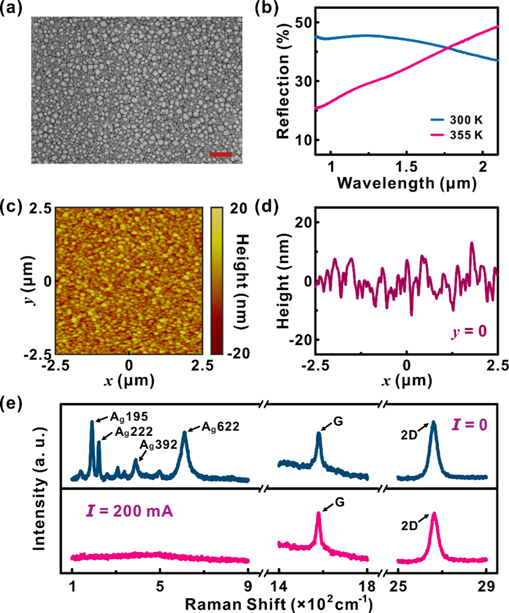
Figure 3. (a) SEM image of the VO2 film fabricated on a glass substrate; the scale bar is 600 nm. (b) Measured reflection spectra of the VO2 film on a glass substrate when it is in the insulating phase and metallic phase. (c) Measured height distribution on the surface of the VO2 film over a square area (5 μm × 5 μm) using the AFM. (d) Height profile at y = 0 in the AFM image. (e) Raman spectra of the electro-tunable optical nanoantennas when the applied current is 0 and 200 mA.
Download figure:
Standard image High-resolution imageNext, the asymmetric dimer nanoantenna was fabricated based on the fabricated VO2 film. We deposited a 50 nm-thick SiO2 film on a 100 nm-thick VO2 film via magnetron sputtering and fabricated the metastructure of the asymmetric gold nanodisk dimer array on the films using electron beam lithography (EBL), EBE, and a subsequent lift-off process. The entire region of the dimer array was a square with an edge length of 100 μm, as shown in figure 4(a). Figure 4(b) shows an SEM image of the asymmetric Au nanodisk dimer array, with periods of 800 and 600 nm in the x- and y-directions, respectively. The details of the asymmetric Au nanodisk dimers are shown in figure 4(c). Note that the diameters of the fabricated Au nanodisk dimers were 240 and 360 nm, and the thickness of both nanodisks was 20 nm. The gap size between the two nanodisks in the dimer could be tuned by precisely controlling the exposure dose in the EBL process. Here, the gap size was set to 25 nm, and the fabrication results were accurate. To realize the electrically tunable phase transition of VO2, a pair of 'T'-shaped Au electrodes were designed near the adjacent sides of the metastructure. The electrodes were fabricated using EBL, EBE, and a lift-off process and the thickness was 20 nm, as shown in figure 4(a). Subsequently, a graphene thin film was transferred onto the asymmetric Au nanodisk dimer array, which was placed in contact with the two 'T'-shaped Au electrodes. The two ends of the electrodes were connected to an external DC source using a conductive silver paste, to establish a loop circuit. The current value in the circuit can be precisely obtained using a built-in amperemeter in the DC source.

Figure 4. (a) Micrograph of the continuously and reversibly electro-tunable asymmetric dimer optical nanoantenna. Here, the metastructure is located in the middle, and an Au electrode pair is fabricated at the both sides of the metastructure; the scale bar is 30 μm. (b) SEM image of the asymmetric Au nanodisk dimer array; the scale bar is 800 nm. (c) SEM image of the details of the asymmetric Au nanodisk dimers; the scale bar is 200 nm. Measured reflection spectra of the asymmetric dimer optical nanoantenna, when the applied current (d) increases from 135 to 195 mA and (e) subsequently decreases from 195 to 135 mA.
Download figure:
Standard image High-resolution imageIn our experiment, we controlled the current from 135 to 195 mA to produce Joule heat in the graphene thin film, which could induce the phase transition of VO2. Meanwhile, we measured the reflection spectra over a wavelength range from 0.9 to 2.1 μm with x-polarized incidence using an FTIR system. First, we kept the VO2 film in the insulating phase, i.e. the applied current value was less than 135 mA, as indicated by the black lines in figures 4(d) and (e). A reflected dip and a resonance peak could be observed in the spectrum, which are marked as (I) and (II), respectively, in figures 4(d) and (e). Next, we increased the current from 135 to 195 mA; the measured reflection spectra are shown in figure 4(d). Notably, the reflection spectrum varied gradually when the applied current increased from 165 mA, and became stable when the current was greater than 185 mA. Because of the good precision of the electrical tunability of this system, several stable intermediate states were obtained as the current increased. We then gradually decreased the current from 195 to 135 mA; the measured reflection spectrum clearly varied when the current was less than 145 mA. The original spectrum was fully recovered when the current reached 135 mA, as shown in figure 4(e). It was found that the variation in the reflection spectra exhibited a hysteresis feature. Notably, the resonance dips and reflected peak in the reflection spectra could also be dynamically and continuously tuned by using the applied current. Next, we performed a quantitative analysis of the continuous tunability of the electro-tuned phase transition of VO2.
3.2. Continuous and reversible modulation of the resonant wavelength
The resonant wavelength is a primary parameter for optical antennas. We first analyzed the continuous and reversible modulation of the resonant wavelengths of the asymmetric dimer nanoantenna, while increasing and decreasing the current. Next, we extracted the resonant wavelengths of the hybrid mode from the reflection spectra, which are indicated by dashed lines (I) in figures 4(d) and (e). We then plotted the variations in the wavelength at the reflected dip positions (λdip) as a function of the increasing and decreasing applied currents, as shown in figure 5(a). As the current increased, the resonant wavelength redshifted continuously from 1.55 to 1.77 μm, resulting from the decrease in the refractive index during the insulator-to-metal phase transition of VO2. Therefore, the wavelength of the resonance dip could be continuously tuned by adjusting the applied current, and its dynamic tunability is reversible. We also extracted the resonant wavelengths of the Fano resonances from the reflection spectra, which are indicated by dashed lines (II) in figures 4(d) and (e). The variations in the wavelength at the resonance peak positions (λpeak), as functions of the increasing and decreasing applied currents, are plotted in figure 5(b). In contrast to the resonance dip, the Fano resonance peak wavelengths were relatively stable, and were maintained at approximately 1.31 μm as the current increased and decreased. This stability of the resonance peak indicates that intensity-only modulation was achieved by applying a current to the optical nanoantenna.
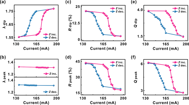
Figure 5. Variations of the resonance wavelength (λ) as functions of the applied current at (a) reflected dip positions and (b) Fano resonance peak positions. Variations of the resonant intensity (R) as functions of the applied current at (e) reflected dip positions and (f) Fano resonance peak positions. Variations of quality factor (Q) as functions of the applied current for (e) reflected dips and (f) Fano resonance peaks. The red and blue lines represent increasing and decreasing currents, respectively.
Download figure:
Standard image High-resolution image3.3. Continuous and reversible modulation of the resonant intensity
We plotted the variations of the reflective intensities at the reflected dip positions (Rdip) and Fano resonant positions (Rpeak) as functions of the increasing and decreasing applied currents, as shown in figures 5(c) and (d), respectively. For the reflected dips, Rdip decreased gradually from 21.7% to 2.5% as the current increased, which could be attributed to the increase in the extinction coefficient during the phase transition process of the VO2 film. These results indicate that the accurate control of the resonant intensity was realized at the hybrid mode position. Notably, this modulation is continuous and reversible. Hysteresis was also formed in the cycling loops. However, it is well known that the Fano resonance in a plasmonic metastructure is sensitive to the surrounding refractive index. This indicates that the Fano resonance will gradually weaken during the phase transition of VO2. Thus, Rpeak also decreased as the current increased from 43.7% to 17.8%, but it can be reversed by decreasing the current. However, λpeak remained almost unchanged during the entire current variation process. Therefore, intensity-only modulation was realized at the Fano resonant positions.
3.4. Continuous and reversible modulation of the quality factor
The quality factor (Q) of resonance is an important parameter for characterizing an optical nanoantenna, providing information concerning the operation bandwidth. We analyzed the modulation of the Q-factor during the current increasing and decreasing processes of the asymmetric dimer nanoantenna. Here, the Q-factors of the hybrid mode (Qdip) and Fano resonance (Qpeak) were extracted; their variations as functions of the increasing and decreasing applied currents are shown in figures 5(e) and (f), respectively. Note that, by increasing the applied current, Qdip continuously decreased from 3.95% to 1.39%, while Qpeak continuously decreased from 6.14% to 2.76%. Both of these properties could be reversed during the current decreasing process. These results were attributed to the variation in the extinction coefficient during the insulator-to-metal transition of the VO2 film.
3.5. Switchability and time response of the device based on electro-tunable phase transition of VO2 film
As demonstrated by the above experimental results, the resonant wavelength, resonant intensity, and quality factor in the reflection spectrum of the optical nanoantenna can be continuously and reversibly tuned by gradually increasing or decreasing the applied current. When current applied cyclically to the optical nanoantenna device from 135 to 195 mA, stable and complete cycling loops for the resonant wavelength, resonant intensity, and quality factor values can be realized. This continuous tunability was attributed to the hysteresis phenomenon during the phase transition of VO2, resulting from the different nucleation processes occurring during the phase transition between the Joule heating and natural cooling processes [46]. Accordingly, the hysteresis width of the VO2 film can also influence the functionality of the optical nanoantenna. Methods such as titanium (Ti)-doping [47] and tungsten (W)-doping [48] can be used to effectively reduce the hysteresis width. For example, the hysteresis width of VO2 may be decreased by 2 °C per at.% of Ti, due to a faster increase of critical temperature in the cooling circle than in the heating circle [47]. Besides, the doping method can also be utilized to adjust the critical temperature of VO2 [48]. These methods provide another method to adjust the electro-tunability of optical nanoantennas.
Notably, the fabricated optical nanoantenna can not only be tuned continuously, but can function in the binary states as well. When the applied current was directly tuned between 0 and 200 mA, the reflection spectrum of the optical nanoantenna underwent an immediate and significant change, thereby indicating that the optical nanoantenna may function between the 'ON' state and 'OFF' state. To further demonstrate the switchability of the graphene-integrated VO2, which has been utilized to realize electro-tunable optical nanoantennas, we used a time-domain reflection system to measure the time response; the experimental results are shown in figure 6(a). Electric currents with square signals were applied to the graphene film, and the modulation frequencies were set as 0.05, 0.10, 0.17, and 0.20 Hz. Note that the amplitude of the modulated signal remained stable when the modulation frequency was less than or equal to 0.10 Hz, indicating a good reversibility during the periodic 'ON' and 'OFF' processes. However, when the modulation frequency increased to 0.20 Hz, the amplitude of the modulated signal decreased, implying that VO2 did not completely return to the insulating phase at this frequency. Next, we extracted a falling edge and a rising edge in figure 6(a) when the modulation frequency was 0.1 Hz, to obtain the 'ON' and 'OFF' switching times, as shown in figures 6(b) and (c), respectively. The switching times taken from the reflection decreasing from 90% to 10% of the maximum value, or vice versa, were defined as the 'ON' switching time (tON) and 'OFF' switching time (tOFF), respectively [49]. Here, the measured 'ON' and 'OFF' switching times for the 0.1 Hz pulses were approximately 510 and 2460 ms, respectively. Compared with the method of directly heating the sample using a heating stage, the electro-tuned phase transition of the graphene-integrated VO2 film, which is achieved by applying a current to the graphene film, exhibited a notable advantage in terms of the modulation time.
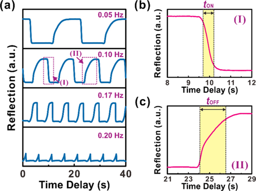
Figure 6. (a) Temporal response of the graphene-integrated VO2 measured at a 0.8 μm wavelength. (b) A falling edge at a modulation frequency of 0.10 Hz; tON represents the 'ON' switching time. (c) A rising edge at a modulation frequency of 0.10 Hz; tOFF represents the 'OFF' switching time.
Download figure:
Standard image High-resolution image3.6. Optical responses of optical nanoantennas with different structural parameters
The optical response of a nanoantenna may be conveniently tuned by adjusting the structural parameters of the subwavelength nanostructures [50]. Two main structural parameters were considered for our asymmetric dimer nanoantennas. The structural asymmetry parameter represents the degree of asymmetry in a dimer nanostructure, which can directly influence the Fano resonance of a nanoantenna device. Furthermore, the gap size of the asymmetric dimer determines the coupling between the two Au nanodisks in a dimer. Here, we designed and fabricated asymmetric dimer nanoantennas with different structural asymmetry parameters. The reflection spectra of these nanoantennas were also measured using the FTIR system at different applied currents. We then simulated the reflection spectra of the asymmetric dimer nanoantennas, having the same structural asymmetry parameter value but different gap sizes.
3.6.1. Structural asymmetry parameter
To analyze the optical responses of the asymmetric dimer nanoantennas with different structural asymmetry parameters, we designed five different nanoantennas. Here, the diameter of one Au nanodisk in the dimers was fixed at 240 nm, while the diameter of the other Au nanodisk varied from 460 to 300 nm. The gap sizes between the two nanodisks were fixed at 25 nm. Based on these structural parameters, we can define the structural asymmetry parameter as δ = |d2 − d1|/d1 × 100%, which is analogous to the definition in literature [51], where d1 and d2 represent the diameters of the Au nanodisks with fixed and variable structural parameters, respectively. Therefore, the δ values of these five nanoantennas were determined to be 91%, 75%, 58%, 42%, and 25%. A smaller δ value indicates a lower degree of asymmetry in the dimer. The simulated reflection spectra of these nanoantennas, when the VO2 film was in the insulating phase and metallic phase, are plotted in figures 7(a) and (b), respectively. These samples were then fabricated, and their reflection spectra were measured using the FTIR system. The measurement results obtained when no current was applied to a sample (i.e., the VO2 film was maintained in the insulating phase) are shown in figure 7(c). The Fano line-type peaks decreased as the structural asymmetry parameter decreased. We then adjusted the applied current to 200 mA, such that the VO2 film was in the metallic phase under these conditions. The measured reflection spectra are shown in figure 7(d). Additionally, all of the Fano line-type peaks disappeared when the VO2 film was induced to the metallic phase using the applied current. Therefore, the electro-switchability of the Fano resonance is universal to asymmetric dimer nanoantennas with different structural asymmetry parameters. Figure 7(e) shows that, when the VO2 film was in the insulating phase, the resonant intensity (Rpeak) at the Fano resonance peak positions continuously decreased from 69.47% to 34.57%; meanwhile, figure 7(f) shows that the resonant wavelength (λpeak) continuously shifted from 1.50 to 1.28 μm as the structural asymmetry parameter decreased from 91% to 25%. Notably, the decrease in the degree of asymmetry led to observable decreases in Rpeak and a blueshift of the λpeak values of the Fano resonances.

Figure 7. Simulated reflection spectra of the asymmetric dimer optical nanoantennas with different structural asymmetry parameters (δ) when the VO2 film is in the (a) insulating phase and (b) metallic phase, respectively. The structural asymmetry parameter is defined as δ = |d2 − d1|/d1 × 100%, where d1 and d2 represent the diameters of the Au nanodisks that have fixed and variable structural parameters, respectively. Measured reflection spectra of the asymmetric dimer optical nanoantennas with different δ values when the VO2 film is in the (c) insulating phase and (d) metallic phase, respectively. Variations of the (e) resonant intensity and (f) resonant wavelength of the Fano resonance peaks as functions of δ.
Download figure:
Standard image High-resolution image3.6.2. Gap size of the asymmetric dimer
Next, we designed several asymmetric dimer nanoantennas with different gap sizes. Here, the diameters of the two Au nanodisks in the dimer were fixed at 240 and 360 nm, and the gap size between the two nanodisks varied from 5 to 40 nm. The simulated reflection spectra of these antennas, when the VO2 film was in the insulating phase and metallic phase are plotted in figures 8(a) and (b), respectively. The reflective intensity of the Fano peak increased as the gap size of the dimer decreased. This could be attributed to the stronger coupling effect between the two adjacent nanodisks when the gap size was less than 10 nm. Figures 8(c) and (d) show the in-plane electric field distributions of the dimers with gap sizes of 5 and 40 nm, respectively, when the VO2 film was in the insulating phase. Notably, the electric field enhancement effect was more remarkable in the dimer with a gap size of 5 nm than that with a gap size of 40 nm, resulting in an increase in the intensity of the Fano resonance. Additionally, when VO2 underwent the phase transition to the metallic phase, the Fano line-type peaks disappeared for all nanoantennas. Therefore, the electro-tunability can be achieved for the asymmetric dimer nanoantennas with different gap sizes. To quantitatively analyze the optical response of the asymmetric dimer nanoantennas with different gap sizes, we extracted the reflection spectra from figure 8(a) for several nanoantennas with different gap sizes. The resonant intensities and resonant wavelengths of the Fano resonance peaks varied as functions of the gap size, which are plotted in figures 8(e) and (f), respectively. Notably, the resonant intensity at the Fano resonance peak positions increased from 60.13% to 70.54%, as the gap size decreased. Meanwhile, the resonant wavelength remained stable at a wavelength of 1.42 μm, as the gap size decreased (indicating a wavelength shift of less than 10 nm). This result indicates that reducing the gap size is an effective method for enhancing the Fano resonance intensity at a specific operating wavelength.

Figure 8. Simulated reflection spectra of the asymmetric dimer optical nanoantennas when the gap size was varied from 5 to 40 nm; the VO2 film is in the (a) insulating phase and (b) metallic phase, respectively. In-plane electric field distributions of the dimers with gap sizes of (c) 5 and (d) 40 nm; the VO2 film is in the insulating phase. Variations of the (e) resonant intensity and (f) resonant wavelength for the Fano resonance peaks as functions of the gap size.
Download figure:
Standard image High-resolution image
4. Discussions and conclusions
In summary, by integrating an asymmetric gold nanodisk dimer array with VO2 and graphene films, we experimentally demonstrated a continuously electro-tunable asymmetric dimer nanoantenna. By accurately controlling the applied electrical current, the Joule heat generated in the graphene film was able to excite the metal–insulator phase transition of the VO2 film. Consequently, the refractive index of VO2 exhibited a relatively large variation. This effect allowed the hybrid mode and Fano effect in the nanodisks to be effectively tuned by varying the applied electrical current. The experimental results showed that the continuous and reversible modulation of the properties of the nanoantenna could be achieved, including the resonant wavelength, resonant intensity, and quality factor (Q-factor). Finally, we varied the gap size and structural asymmetry parameter of the nanodisk dimer to expand the modulation range. It was shown that the resonant intensity is stronger with a smaller gap size. Moreover, the resonant wavelength underwent a redshift when the structural asymmetry parameter was increased. Compared with the traditional thermal modulation of VO2, electrical modulation has a higher operation speed and better compatibility, thereby increasing the number of potential applications of our proposed nanoantennas. Additionally, the excited Fano resonance is sensitive to the change of refractive index. Combining the dynamic optical nanoantenna design with such a specific physical effect, we may further improve its performance especially for high-quality factors and enhanced emission intensity. Notably, the electro-tunable optical nanoantennas were realized in this study over a wavelength range of 0.9–2.1 μm, which completely covers the range of near-infrared optical communication bands (1.260–1.675 μm) [52]. We anticipate that such electro-tunable optical nanoantennas may provide significant inspiration for the development of fiber optics technologies and optical information science. We believe that the results of this study provide a new method for achieving electro-tunable optical nanoantennas for various applications including optical communications, information storage and encryption, and photoelectric sensors.
Acknowledgments
This work was supported by the National Key R&D Program of China (2020YFA0211300, 2017YFA0303702), and the National Natural Science Foundation of China (Grant Nos. 11634005, 61975078 and 11974177).
Data availability statement
All data that support the findings of this study are included within the article (and any supplementary files).